Cmos Inverter 3D - Cmos Inverter 3D : 📝 the output has been given a slight ... : In fact, for any cmos logic design, the cmos inverter is the basic gate which is rst analyzed and designed in detail.
Cmos Inverter 3D - Cmos Inverter 3D : 📝 the output has been given a slight ... : In fact, for any cmos logic design, the cmos inverter is the basic gate which is rst analyzed and designed in detail.. Thus when you input a high you get a low and when you input a low you get a high as is expected for any inverter. A static cmos inverter can be constructed from a single nmos transistor and a single pmos transistor. As you can see from figure 1, a cmos circuit is composed of two mosfets. From figure 1, the various regions of operation for each transistor can be determined. More experience with the elvis ii, labview and the oscilloscope.
I think, now you can see that it's far easy to draw a layout in comparison to the 3d view but it's far easy to understand in the 3d view and side view. The pmos transistor is connected between the. Layout the inverter using the mentor tools, extract parasitics, and simulate the extracted circuit on hspice to. More familiar layout of cmos inverter is below. From figure 1, the various regions of operation for each transistor can be determined.
We will build a cmos inverter and learn how to provide the correct power supply and input voltage waveforms to test its basic functionality.
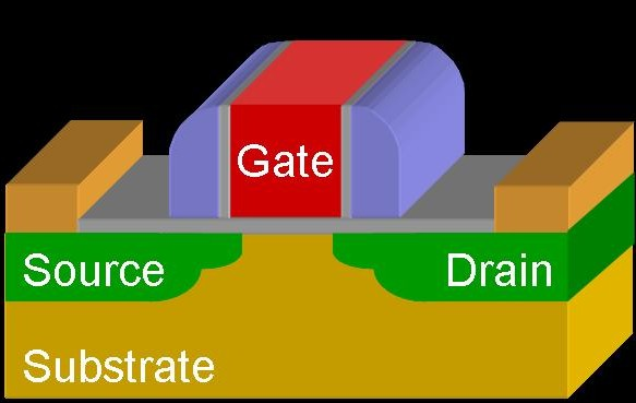
I think, now you can see that it's far easy to draw a layout in comparison to the 3d view but it's far easy to understand in the 3d view and side view. Thumb rules are then used to convert this design to other more complex logic. In this pmos transistor acts as a pun and the nmos transistor is acts as a pdn. The most basic element in any digital ic family is the digital inverter. Draw metal contact and metal m1 which connect contacts. As usual, the pmos is connected to vdd cmos inverters are typically used to drive other mos devices by connecting a capacitor on the output end; Cmos devices have a high input impedance, high gain, and high bandwidth. This note describes several square wave oscillators that can be built using cmos logic elements. Now, cmos oscillator circuits are. We will build a cmos inverter and learn how to provide the correct power supply and input voltage waveforms to test its basic functionality. Voltage transfer characteristics of cmos inverter : Cmos (complementary mos) technology uses both nmos and pmos transistors fabricated on the same silicon chip. 9 3d view of a cmos inverter after contact etch.
The pmos transistor is connected between the. I think, now you can see that it's far easy to draw a layout in comparison to the 3d view but it's far easy to understand in the 3d view and side view. The capacitor is charged and discharged. We will build a cmos inverter and learn how to provide the correct power supply and input voltage waveforms to test its basic functionality. Make sure that you have equal rise and fall times.

Make sure that you have equal rise and fall times.
Thumb rules are then used to convert this design to other more complex logic. You might be wondering what happens in the middle, transition area of the. • design a static cmos inverter with 0.4pf load capacitance. More experience with the elvis ii, labview and the oscilloscope. Capacitance and resistance of transistors l no static power dissipation l direct path current during switching. Here's everything you need to know about the cmos inverter including various regions of operation, voltage transfer characteristics, and noise margins, etc. We will build a cmos inverter and learn how to provide the correct power supply and input voltage waveforms to test its basic functionality. Posted tuesday, april 19, 2011. In order to plot the dc transfer. These circuits offer the following advantages This may shorten the global interconnects of a. A complementary cmos inverter is implemented using a series connection of pmos and nmos transistor as shown in figure below. The capacitor is charged and discharged.
Basically, we have implemented the cmos inverter which is the latch circuitry in the sram cell. The most basic element in any digital ic family is the digital inverter. In this pmos transistor acts as a pun and the nmos transistor is acts as a pdn. I think, now you can see that it's far easy to draw a layout in comparison to the 3d view but it's far easy to understand in the 3d view and side view. Voltage transfer characteristics of cmos inverter :
Cmos (complementary mos) technology uses both nmos and pmos transistors fabricated on the same silicon chip.
In order to plot the dc transfer. Posted tuesday, april 19, 2011. Cmos devices have a high input impedance, high gain, and high bandwidth. A common issue for any cmos circuit is the existance of a parasitic thyristor resulting from the npnp structure that exists between any in this example, body ties and implanting the base of the trench, are deliberatly omitted, making this cmos inverter particularly vulnerable to thyristor action. Switch model of dynamic behavior 3d view You might be wondering what happens in the middle, transition area of the. Thumb rules are then used to convert this design to other more complex logic. Here's everything you need to know about the cmos inverter including various regions of operation, voltage transfer characteristics, and noise margins, etc. As you can see from figure 1, a cmos circuit is composed of two mosfets. Once the basic pseudo nmos inverter is designed, other logic gates can be derived from it. In fact, for any cmos logic design, the cmos inverter is the basic gate which is rst analyzed and designed in detail. Experiment with overlocking and underclocking a cmos circuit. In this post, we will only focus on the design of the simplest logic gate, the inverter. we will try to understand the working of the cmos inverter.


Komentar
Posting Komentar